Characteristics of 2SD261 Transistor
- Type: NPN
- Collector-Emitter Voltage, max: 20 V
- Collector-Base Voltage, max: 40 V
- Emitter-Base Voltage, max: 5 V
- Collector Current − Continuous, max: 0.5 A
- Collector Dissipation: 0.5 W
- DC Current Gain (hfe): 40 to 400
- Operating and Storage Junction Temperature Range: -55 to +150 °C
- Package: TO-92
Pinout of 2SD261
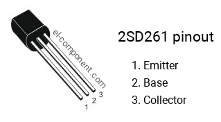
The 2SD261 is manufactured in a plastic TO-92 case. When looking at the flat side with the leads pointed downward, the three leads emerging from the transistor are, from left to right, the emitter, base, and collector leads.
Here is an image showing the pin diagram of this transistor.
Classification of hFE
The 2SD261 transistor can have a current gain of
40 to
400. The gain of the
2SD261G will be in the range from
200 to
400, for the
2SD261O it will be in the range from
70 to
140, for the
2SD261R it will be in the range from
40 to
80, for the
2SD261Y it will be in the range from
120 to
240.
Marking
Sometimes the "2S" prefix is not marked on the package - the 2SD261 might only be marked "
D261".
Complementary PNP transistor
The complementary
PNP transistor to the 2SD261 is the
2SA643.
2SD261 Transistor in TO-92 Package
The
KSD261 is the TO-92 version of the 2SD261.
Replacement and Equivalent for 2SD261 transistor
You can replace the 2SD261 with the
MPS3706 or
MPS6532.
If you find an error please send an email to mail@el-component.com
