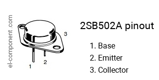
2SB502A Bipolar Transistor
Characteristics of 2SB502A Transistor
- Type: PNP
- Collector-Emitter Voltage, max: -80 V
- Collector-Base Voltage, max: -110 V
- Emitter-Base Voltage, max: -10 V
- Collector Current − Continuous, max: -3 A
- Collector Dissipation: 25 W
- DC Current Gain (hfe): 30 to 280
- Transition Frequency, min: 5 MHz
- Operating and Storage Junction Temperature Range: -65 to +150 °C
- Package: TO-66
Pinout of 2SB502A
Classification of hFE
Marking
Complementary NPN transistor
If you find an error please send an email to mail@el-component.com
